Welcome to Minghui's official website - PCB Manufacturing's 10-year major brand
Mobile phone:19168988006wu@mhfpcb.com
Welcome to Minghui's official website - PCB Manufacturing's 10-year major brand
Mobile phone:19168988006wu@mhfpcb.com

| Process | project | Content | Conventional | Illustration |
| Cutting and splicing | Cutting and completing plate thickness | Number of layers | 2-6 layers (layered board) | 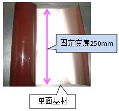 |
| 2-10 layers (soft hard bonding board) | ||||
| Floors 1-8 (soft board) | ||||
| Cutting and splicing dimensions | 250*(220~400)mm 500*(220~400)mm |
|||
| Complete board size (maximum) | 480mm*380mm | |||
| Complete board size (minimum) | 5mm*8mm | |||
| Maximum sheet thickness (double-sided copper) | 0.3mm | |||
| Minimum sheet thickness (single-sided copper content) | 0.05mm (finished product) | |||
| Other auxiliary materials | Specification of pressure-sensitive adhesive material | Pressure sensitive adhesive: 30/50/100/130um |
 |
|
| Specification of thermosetting adhesive material | Thermosetting adhesive: 12.5/15/25/40/50um | |||
| PI reinforcement (excluding adhesive) material specifications | PI:1.0 - 13mil | |||
| PET reinforcement (excluding adhesive) material specifications | White: 0.05-0.25mm | |||
| Transparent: 0.025-0.25mm | ||||
| FR-4 reinforcement (excluding adhesive) material specifications | FR-4:≥50um | |||
| Other types of reinforcement materials | Stainless steel, aluminum plate, nickel steel sheet according to customer requirements | |||
| Common board materials | Material type | Single and double-sided adhesive Single and double-sided adhesive free and halogen-free Single and double-sided adhesive without halogen |
 |
|
| Copper thickness of substrate (electrolytic or rolled) | 1/3oz 1/2oz 1oz 2oz | |||
| Substrate PI | 0.5mil,0.7mil,0.8mil, 1mil,2mil |
| working procedure | project | Content | Conventional | Illustration | ||||||||||||||||||||||||||||||||
| Working edge size | Double sided tin deposition, gold deposition OSP、 Tinplate | TD direction 10/6mm, MD direction 6mm (The clamp is fixed on the TD edge, 10mm) |
 |
|||||||||||||||||||||||||||||||||
| Single and double-sided electric gold plates (250mm direction) | 7mm | |||||||||||||||||||||||||||||||||||
| Single sided tin deposition, gold deposition, OSP board | Long side/short side ≥ 6mm | |||||||||||||||||||||||||||||||||||
| TFT products with fine fingers facing outward | Long/short side ≥ 7mm, and the clamping edge of TD side ≥ 10mm | |||||||||||||||||||||||||||||||||||
| Multi layer soft hard composite board | Long side/short side ≥ 12mm | |||||||||||||||||||||||||||||||||||
| drill hole | Drilling tolerance | Positioning tolerance | One drilling: ± 0.05mm | 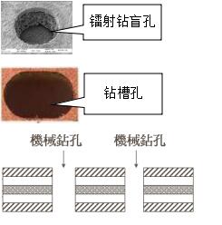 |
||||||||||||||||||||||||||||||||
| Secondary drilling: ± 0.1mm | ||||||||||||||||||||||||||||||||||||
| Laser drilling (minimum blind hole) | Ø0.08mm | |||||||||||||||||||||||||||||||||||
| Laser drilling (minimum through-hole) | Ø0.05mm | |||||||||||||||||||||||||||||||||||
| Mechanical drilling aperture (minimum) | Ø0.1mm | |||||||||||||||||||||||||||||||||||
| Mechanical drilling aperture (maximum drill bit) | Ø6.30mm | |||||||||||||||||||||||||||||||||||
| Drilling hole (minimum) | Ø0.60mm | |||||||||||||||||||||||||||||||||||
| Finished hole diameter tolerance (plated through-hole) | ±2mil(±0.05mm) | |||||||||||||||||||||||||||||||||||
| Finished hole diameter tolerance (non plated through-hole) | ±1mil(±0.025mm) | |||||||||||||||||||||||||||||||||||
| Metalization of holes | Black hole PTH / electroplate |
Minimum average copper thickness of PTH hole wall | Double sided panel: 10-18um | 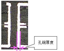 |
||||||||||||||||||||||||||||||||
| Module board (TFT): 8-15um | ||||||||||||||||||||||||||||||||||||
| Soft hard combination board: ≥ 20um | ||||||||||||||||||||||||||||||||||||
| Soft board multi-layer layered board: ≥ 16um | ||||||||||||||||||||||||||||||||||||
| Control according to customer's special requirements | ||||||||||||||||||||||||||||||||||||
| Producible size | 250 or 500 * (220-400) mm | |||||||||||||||||||||||||||||||||||
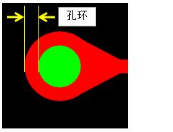
| Graphic circuit | Minimum line width/line gap of film | Minimum hole ring (calculated within the inner layer of multi-layer board) | Limit 0.075mm (single and double-sided panels) Conventional 0.1mm Safety value 0.12mm |
 |
||||||||||||||||||||||||||||||||
| Unilateral 0.15mm (3, 4 layers), safety value 0.2mm | ||||||||||||||||||||||||||||||||||||
| Unilateral 0.25mm (5, 6 layer board), safety value 0.3mm | ||||||||||||||||||||||||||||||||||||
| Unilateral 0.35mm (6 or more layers) | ||||||||||||||||||||||||||||||||||||
| Minimum hole ring (outer layer of multi-layer board) | Unilateral 0.1mm, safety value 0.15mm | |||||||||||||||||||||||||||||||||||
| Process | project | Content | Conventional | Illustration | ||||||||||||||||||||||||||||||||
| Graphic circuit | Minimum line width/line gap of film | Minimum distance from NPTH hole to line | 0.1mm, safety value 0.2mm (drilling) |  |
||||||||||||||||||||||||||||||||
| 0.15mm, safety value 0.25mm (steel die punching) | ||||||||||||||||||||||||||||||||||||
| Minimum line width/gap of 1/3 OZ copper base | 0.05/0.04mm (line compensated) | |||||||||||||||||||||||||||||||||||
| Minimum line width/gap of 1/2 OZ copper base | 0.06/0.07mm (line compensated) | |||||||||||||||||||||||||||||||||||
| Minimum line width/gap of 1OZ bottom copper | Single panel: 0.07/0.08mm (line compensated) | |||||||||||||||||||||||||||||||||||
| Double sided board: 0.08/0.09mm (compensated circuit) | ||||||||||||||||||||||||||||||||||||
| Minimum line width and spacing of the outer layer of the soft hard composite board | 0.11/0.09mm (line compensated) | |||||||||||||||||||||||||||||||||||
| Minimum line width/line gap of multi-layer soft board | 0.09/0.07mm (line compensated) | |||||||||||||||||||||||||||||||||||
| Etching compensation (overall): 1 OZ copper | 0.03-0.04mm | |||||||||||||||||||||||||||||||||||
| Etching compensation (overall): 1/2 OZ copper | 0.02-0.03mm | |||||||||||||||||||||||||||||||||||
| Etching compensation (overall): 1/3 OZ copper | 0.015-0.02mm | |||||||||||||||||||||||||||||||||||
| Note: All independent lines shall be increased by 0.01-0.02mm (overall) on the basis of overall compensation; Minimum line spacing of 0.04mm | ||||||||||||||||||||||||||||||||||||
| Dry film | Alignment tolerance | ±0.05mm | 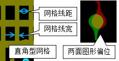 |
|||||||||||||||||||||||||||||||||
| Deviation of two-sided graphics (alignment overlap) | ±0.05mm | |||||||||||||||||||||||||||||||||||
| Minimum Grid (Area) | 0.2 × 0.2mm (preferably at a 45 ° angle) | |||||||||||||||||||||||||||||||||||
| Minimum grid line width/line spacing | 0.15/0.15mm | |||||||||||||||||||||||||||||||||||
| Solder mask | Solder mask | Minimum distance from window to solder pad on one side | 0.05mm, safe value 0.075mm | 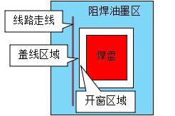 |
||||||||||||||||||||||||||||||||
| Minimum width of green oil bridge | 0.1mm | |||||||||||||||||||||||||||||||||||
| Green Oil Bridge Cover Line with Large Single Side | 0.05mm, safe value 0.075mm | |||||||||||||||||||||||||||||||||||
| Green minimum window | Ø 0.025mm, safety value Ø 0.04mm | |||||||||||||||||||||||||||||||||||
| Ink thickness | ≥ 10um (usually 9-25um, Guanpin thermosetting oil: 9-15UM |
|||||||||||||||||||||||||||||||||||
| Minimum negative letter height/minimum line width for green oil | 1.0/0.15mm | |||||||||||||||||||||||||||||||||||
| character | character | Minimum line width for positive text | 0.1mm, safe value 0.13mm |  |
||||||||||||||||||||||||||||||||
| Minimum line width for negative text | 0.125mm, safety value 0.15mm | |||||||||||||||||||||||||||||||||||
| Minimum height of text | 0.8mm | |||||||||||||||||||||||||||||||||||
| Minimum width of text | 0.8mm | |||||||||||||||||||||||||||||||||||
| Process | project | Content | Conventional | Illustration | ||||||||||||||||||||||||||||||||
| character | Minimum distance from characters to solder pads | 0.15mm, safety value 0.25mm | 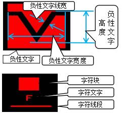 |
|||||||||||||||||||||||||||||||||
| Minimum line width of character line segments (non text) | 0.1mm, optimal value 0.2mm | |||||||||||||||||||||||||||||||||||
| The minimum distance between character blocks and solder pads on one side | ≥0.2mm | |||||||||||||||||||||||||||||||||||
| Minimum distance from characters to appearance | 0.25mm | |||||||||||||||||||||||||||||||||||
| Carbon oil | Minimum carbon oil width/carbon oil spacing | 0.25/0.3mm | ||||||||||||||||||||||||||||||||||
| Minimum distance from the outer edge | 0.3mm | |||||||||||||||||||||||||||||||||||
| Carbon oil resistance tolerance (3000 Ω high resistance) | ±400Ω | |||||||||||||||||||||||||||||||||||
| ACP Conductive adhesive |
ACP thickness range | 15-25um | ||||||||||||||||||||||||||||||||||
| Number of conductive particles | > 30 pieces/mm ² | |||||||||||||||||||||||||||||||||||
| punching | punching | Drilling accuracy tolerance | ±1mil(0.025mm) | |||||||||||||||||||||||||||||||||
| Fit together | Cover film processing | Minimum drilling hole for covering film window opening | Ø 0.4mm (drilling processing), Safety value Ø 0.7mm |
 |
||||||||||||||||||||||||||||||||
| Minimum square window for covering film windows | 0.6 × 0.6mm (steel mold processing) | |||||||||||||||||||||||||||||||||||
| 0.5 × 0.5mm (precision die processing) | ||||||||||||||||||||||||||||||||||||
| Minimum window spacing for covering film | 0.5mm (precision mold), 0.2mm (laser engraving) | |||||||||||||||||||||||||||||||||||
| 0.15mm (ordinary drilling) | ||||||||||||||||||||||||||||||||||||
| 0.2mm (slot, cross COV drilling bridge) | ||||||||||||||||||||||||||||||||||||
| Minimum aperture for cutting cover film | 0.7mm | |||||||||||||||||||||||||||||||||||
| Minimum aperture for cutting thermosetting adhesive and double-sided adhesive | 1.0mm | |||||||||||||||||||||||||||||||||||
| Minimum window spacing for cutting cover film with cutting machine | 0.15mm | |||||||||||||||||||||||||||||||||||
| Minimum window for cutting cover film with cutting machine | 0.6*0.6mm | |||||||||||||||||||||||||||||||||||
| Minimum punching of covering film | 0.6mm (steel mold processing) | |||||||||||||||||||||||||||||||||||
| Double sided adhesive window opening is larger than single-sided FPC | 0.3-0.5mm | |||||||||||||||||||||||||||||||||||
| Distance from the edge of the cover film window to the edge of the solder pad or circuit | Products below 250 × 230mm: 0.05mm (safety value 0.1mm) Products above 250 × 230mm: 0.075mm (safety value 0.15mm) | |||||||||||||||||||||||||||||||||||
| Alignment tolerance of covering film and auxiliary materials | ± 0.15mm, safety value ± 0.2mm | |||||||||||||||||||||||||||||||||||
| Excess glue amount of covering film (unilateral) | Conventional 0.08-0.12mm Limit 0.03mm (TPX compression) |
|||||||||||||||||||||||||||||||||||
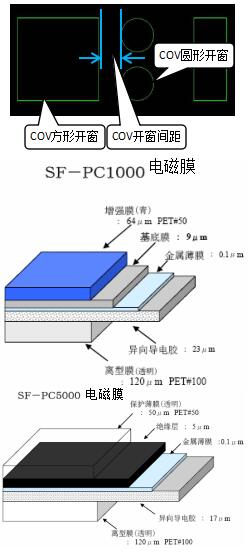
| Electromagnetic film | SF-PC5000/5500/5900 black electromagnetic film minus release film thickness | 22um/22um/9um | ||||||||||||||||||||||||||||||||||
| Process | project | Content | Conventional | Illustration | ||||||||||||||||||||||||||||||||
| Fit together | Electromagnetic film | SF-PC1000 silver electromagnetic film minus release film thickness | 32.1um | 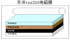 |
||||||||||||||||||||||||||||||||
| TSS200/TSS100 black electromagnetic film | 22um/12um | |||||||||||||||||||||||||||||||||||
| electroplate | surface treatment | Nickel plating thickness | 2.54-9um (conventional value 2-6um) | 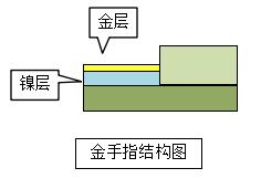 |
||||||||||||||||||||||||||||||||
| Plating thickness | 0.025-0.2um (Normal value 0.025-0.075um) |
|||||||||||||||||||||||||||||||||||
| Nickel deposition thickness | 1-6um (conventional 1-3um or 2-5um) | |||||||||||||||||||||||||||||||||||
| Thickness of gold deposition | 0.025-0.125um (Normal value 0.025-0.075um) |
|||||||||||||||||||||||||||||||||||
| Tin plating thickness | 3-10um | |||||||||||||||||||||||||||||||||||
| Tin deposition thickness | 0.6-1.2um | |||||||||||||||||||||||||||||||||||
| OSP thickness | 0.3-0.5um | |||||||||||||||||||||||||||||||||||
| Control according to customer's special requirements | ||||||||||||||||||||||||||||||||||||
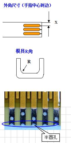
| Punching and cutting | Exterior cutting | Outline Tolerance | ± 0.05mm (high-precision mold) ± 0.07mm (precision mold, etching knife mold) ± 0.1mm (ordinary steel mold, simple steel mold) ± 0.2mm (ordinary die) |
 |
||||||||||||||||||||||||||||||||
| Outer corner dimension (finger center to edge) tolerance | ± 0.05mm (high-precision mold) ± 0.07mm (precision mold making) |
|||||||||||||||||||||||||||||||||||
| ± 0.1mm (for ordinary steel mold production and etching knife mold) | ||||||||||||||||||||||||||||||||||||
| Sharp corners of the appearance are allowed to use transition rounded corners | R≥0.20mm | |||||||||||||||||||||||||||||||||||
| The minimum distance between the center of the positioning hole and the outer edge | 2mm | |||||||||||||||||||||||||||||||||||
| Minimum distance between units | ≥ 0.5mm (suitable for jumping, usually 1-2mm) | |||||||||||||||||||||||||||||||||||
| Boundary distance cutting line | ≥ 2.0mm (die), ≥ 2.5mm (handmade) | |||||||||||||||||||||||||||||||||||
| Positioning hole (Ø 2.0mm) center distance from cutting line | ≥ 2.5mm (die), ≥ 3mm (handmade) | |||||||||||||||||||||||||||||||||||
| Minimum diameter of semi-circular hole | 0.25mm, safety value 0.3mm | |||||||||||||||||||||||||||||||||||
| Minimum distance from circuit to board edge | 0.40mm (hand cut) | |||||||||||||||||||||||||||||||||||
| 0.3mm (ordinary knife mold) | ||||||||||||||||||||||||||||||||||||
| 0.15mm (steel mold, etching knife mold) | ||||||||||||||||||||||||||||||||||||
| 0.1mm (precision die) | ||||||||||||||||||||||||||||||||||||
| Process | project | Content | Conventional | Illustration | ||||||||||||||||||||||||||||||||
| Punching and cutting | Exterior cutting | The minimum distance from the circuit to the board edge is 500mm, and there is no gap in the board arrangement | 0.3mm (die) | |||||||||||||||||||||||||||||||||
| V-cut Milling plate V-CUT |
Soft hard combination board | Diameter of gong and knife | Minimum Ø 0.8mm (minimum inner arc radius R0.4mm) | 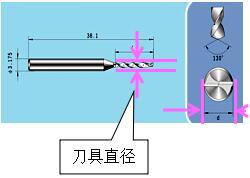 |
||||||||||||||||||||||||||||||||
| Pipe position hole | NPTH hole Ø 1.0mm | |||||||||||||||||||||||||||||||||||
| tolerance | Milling plate peripheral tolerance ± 0.13mm | |||||||||||||||||||||||||||||||||||
| Minimum distance from circuit to board edge | 0.2mm (gong edge) | |||||||||||||||||||||||||||||||||||
| FR4 with the thinnest total thickness of V-CUT | 0.3mm | |||||||||||||||||||||||||||||||||||
| The shallowest depth of V-CUT | 0.08mm (oblique angle: 45 °) | |||||||||||||||||||||||||||||||||||
| test | Flying needle test | Minimum line width/spacing for flying needle test | 0.05/0.05mm | |||||||||||||||||||||||||||||||||
| Maximum height difference of test points | 1.5mm | |||||||||||||||||||||||||||||||||||
| Finished product thickness | Finished product thickness | Finished product thickness tolerance (0.05-0.10mm) | ±0.015mm | 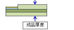 |
||||||||||||||||||||||||||||||||
| Finished product thickness tolerance (0.11-0.2mm) | ±0.02mm | |||||||||||||||||||||||||||||||||||
| Finished product thickness tolerance (0.21-0.40mm) | ±0.03mm | |||||||||||||||||||||||||||||||||||
| Multi layer soft hard composite board | Based on the specific layout structure | |||||||||||||||||||||||||||||||||||
| impedance | Impedance tolerance | Single point impedance tolerance | ﹢/-10% | |||||||||||||||||||||||||||||||||
| Differential impedance tolerance | ﹢/-10% | |||||||||||||||||||||||||||||||||||
| Board type | Double sided panel (100/-10 ohms) | 1MIL 1/3OZ non adhesive material 1.5MIL 1/3OZ non adhesive material 1/2MIL 1/3OZ with adhesive material |
||||||||||||||||||||||||||||||||||
| Multi-layer board | Match according to actual materials | |||||||||||||||||||||||||||||||||||
| SMT | SMT | Anti static level | class a | 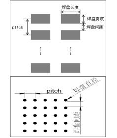 |
||||||||||||||||||||||||||||||||
| Dust free grade | 100000 level | |||||||||||||||||||||||||||||||||||
| Minimum component | Conventional 0201, Extreme 01005 | |||||||||||||||||||||||||||||||||||
| Minimum component spacing | Conventional 0.3mm, maximum 0.2mm | |||||||||||||||||||||||||||||||||||
| Minimum IC pitch | 0.3mm | |||||||||||||||||||||||||||||||||||
| Minimum connector pitch | 0.3mm | |||||||||||||||||||||||||||||||||||
| Minimum BGA pitch | 0.3mm | |||||||||||||||||||||||||||||||||||
| Maximum layout size | Conventional 250 * 240mm limit 330 * 240mm | |||||||||||||||||||||||||||||||||||
| Maximum board surface step | Conventional ≤ 0.3mm Limit ≤ 0.35mm | |||||||||||||||||||||||||||||||||||
| Printing solder paste type | Lead free and halogen-free | |||||||||||||||||||||||||||||||||||
| Thickness of solder paste printing | 120-180um | |||||||||||||||||||||||||||||||||||
| Process | project | Content | Conventional | Illustration |
| SMT | SMT | Minimum tinned area | 0.3*0.25mm | 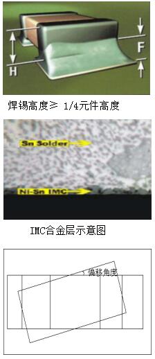 |
| Solder height | Component height above 1/4 | |||
| Tin height on component pins | Greater than 1/2 of the component pin | |||
| IMC alloy layer thickness | 1-3um | |||
| Number of temperature zones for hot air reflow soldering | 10 temperature zones | |||
| Reflow soldering temperature | Maximum 250 ℃ | |||
| Manual welding temperature | 280-320℃ | |||
| Deviation tolerance of surface mount devices | ±50um | |||
| Connector alignment tolerance | ±50um | |||
| IC alignment tolerance | ±50um | |||
| LED alignment tolerance | ±50um | |||
| LED offset angle | 1° | |||
| LED parallelism tolerance | ±50um | |||
| AOI inspection capability | General: CHIP minimum: 0201, IC spacing: pitch=0.3mm; Limit: CHIP Minimum: 01005, IC spacing: pitch=0.3mm |
|||
| ICT testing | 1200 points | |||
| glue | UV glue, thermosetting glue, underfill (bottom filling) | |||
| Excess glue tolerance for dispensing (dispensing side) | ±50um | |||
| Excess glue tolerance for dispensing (non dispensing side) | ±50um |

Telephone
TOP